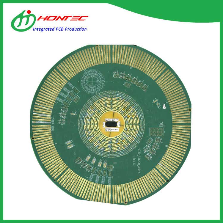
How to build a multilayer board?
2023-10-17
Building a multilayer board requires a combination of design, fabrication, and assembly processes. Here is a general overview of the steps involved in building a multilayer board:
1. Design Stage:
Determine the circuit requirements and functionality of the board.
Create a schematic diagram of the circuit, including component placement and interconnections.
Perform layout design, including trace routing, layer assignment, and signal integrity considerations.
Ensure proper power and ground plane distribution, controlled impedance, and signal isolation.
2. Fabrication Stage:
Prepare the base material, typically fiberglass-reinforced epoxy resin (FR-4) laminates, in the desired thickness.
Clean the base material to remove any contaminants or residues.
Apply a layer of copper foil to the top and bottom surfaces of the base material.
Use photoresist and a photomask to transfer the circuit pattern onto the copper foils through a process called photolithography.
Etch away the unwanted copper using an etchant, leaving behind the desired conductive traces.
Repeat the process for each additional layer of the board, aligning the layers and stacking them together.
3. Drilling and Plating:
Drill holes or vias through the stacked layers to establish electrical connections between different layers.
Clean the drilled holes to remove debris or contaminants.
Electroplate the holes with a conductive material, typically copper, to create conductive pathways between the layers.
4. Lamination:
Apply heat and pressure to the stacked layers to bond them together using heat-activated adhesive materials called prepreg.
Ensure proper alignment and registration of the layers during lamination to maintain accuracy and integrity.
5. Surface Finishing:
Apply a protective layer over the exposed copper surfaces to prevent oxidation and ensure solderability. Common surface finishes include solder mask and gold plating.
6. Component Assembly:
Place and solder the electronic components onto the board, following the design layout and using appropriate soldering techniques (e.g., surface mount technology or through-hole soldering).
Inspect and test the assembled board for proper functionality and electrical connectivity.
It's important to note that building a multilayer board requires specialized knowledge, expertise, and access to the necessary equipment and materials. The process may vary depending on the specific requirements, complexity, and manufacturing capabilities available. It is often performed by professional PCB manufacturers or specialized assembly houses with the necessary expertise and infrastructure.
For individuals or small-scale projects, it may be more practical to outsource the fabrication of multilayer boards to experienced PCB manufacturers who can handle the entire process, from design review to final assembly and testing.


