
Understanding PCB Fabrication: The Heart of Modern Electronics Manufacturing
2025-06-12
Printed Circuit Boards (PCBs) are the backbone of nearly every electronic device we use today — from smartphones and laptops to medical equipment and automotive systems. But have you ever wondered how these intricate boards are made? The process of PCB fabrication turns raw materials into the complex circuits that power modern technology.
What Is PCB Fabrication?
PCB fabrication refers to the manufacturing process of creating printed circuit boards. It involves a series of precise steps that convert design files into physical boards with conductive pathways, components, and protective layers. This process ensures that the final product functions reliably and efficiently in its intended application.
The PCB Fabrication Process: Step-by-Step
1. Design and Printing: The process starts with the PCB layout design using specialized software. The design is printed onto a transparent film, which acts as a blueprint for the circuit.
2. Substrate Preparation: The base material, often made of fiberglass (FR4), is cleaned and prepared. This substrate provides mechanical support for the circuit.
3. Copper Cladding: A thin layer of copper foil is laminated onto the substrate. This copper will form the conductive traces.
4. Photoresist Application: A photosensitive film called photoresist is applied over the copper. This layer protects parts of the copper during etching.
5. UV Exposure and Developing: The printed film is aligned with the photoresist, and ultraviolet (UV) light exposes the design onto the board. Areas exposed to UV harden, while unexposed areas remain soft.
6. Etching: The board is submerged in a chemical bath that removes the unprotected copper, leaving behind only the desired circuit pattern.
7. Drilling: Precise holes for vias and component leads are drilled using computer-controlled machines.
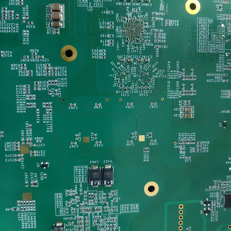
8. Plating and Coating: Holes are plated with copper to create electrical connections between layers. Then, protective solder masks and silkscreens are applied to insulate and label the board.
9. Testing and Quality Control: The finished PCB undergoes electrical testing to check for shorts, opens, and other defects.
Types of PCBs Fabricated
Single-Sided: Copper on one side only, used for simple circuits.
Double-Sided: Copper on both sides, with vias connecting layers.
Multilayer: Multiple copper layers separated by insulating material for complex designs.
Why Is PCB Fabrication Important?
Precision: Ensures electrical paths are accurate for reliable device performance.
Durability: Proper fabrication improves mechanical strength and resistance to environmental factors.
Customization: Enables unique designs for specialized electronics.
Scalability: Supports mass production of consistent, high-quality boards.
Challenges in PCB Fabrication
Miniaturization: As devices shrink, PCBs must be fabricated with finer features and tighter tolerances.
Material Selection: Choosing substrates and coatings that withstand heat, moisture, and mechanical stress.
Cost Efficiency: Balancing quality with affordable production costs.
Conclusion
PCB fabrication is a sophisticated blend of art and science that transforms circuit designs into physical, functional boards essential to today’s electronics. Whether for consumer gadgets, industrial machinery, or cutting-edge technology, understanding this process helps appreciate the complexity behind every electronic device we rely on.